Why in news?
The foundation stone for India's first advanced 3D chip packaging unit was laid in Bhubaneswar, Odisha. Approved under the India Semiconductor Mission (ISM) at a cost of ₹1,934 crore, the facility is led by US-based 3D Glass Solutions and has received investments from Intel, Lockheed Martin, and other venture capital and private equity funds.
It is being described as the project that will put India "at the cutting edge of technology" in advanced chip packaging.
What’s in Today’s Article?
- What are Semiconductors and Why Do They Matter?
- Moore's Law and its Limitations
- Traditional Chips vs. 3D Glass Chips — What's the Difference
- About the Odisha Facility
- India Semiconductor Mission (ISM) — Overview
- ISM 2.0 — What's Next?
- Conclusion
What are Semiconductors and Why Do They Matter
- A semiconductor is a material (usually silicon) that can conduct electricity under certain conditions — making it the foundation of all modern electronics, from smartphones and laptops to missiles and satellites.
- Chips (or integrated circuits) are tiny devices made from semiconductors that process and store information.
- Every digital device —phone, car, ATM — runs on chips. Countries that can design and manufacture chips hold enormous technological, economic, and strategic power.
Moore's Law and its Limitations
- Moore's Law, formulated in 1965 by Gordon Moore (co-founder of Intel), states that the number of transistors on a chip doubles approximately every two years, driving exponential improvements in computing power while reducing costs.
- For decades, this was the guiding principle of the semiconductor industry — chips kept getting smaller, faster, and cheaper.
- However, chips are now approaching physical and thermal limits — one simply cannot keep shrinking transistors indefinitely.
- As a result, the industry is now pursuing alternative strategies to sustain performance improvements — the most promising of which are advanced packaging, chiplets, and 3D integration.
Traditional Chips vs. 3D Glass Chips — What's the Difference
- Traditional chips are built on silicon wafers, with all components arranged side by side on a flat, planar surface.
- This works well up to a point, but as one tries to fit more and more components onto the same flat surface, he/she inevitably hit physical limits.
- There is only so much space on a single layer, and beyond a certain point, components simply cannot be made any smaller or packed any tighter without causing errors, overheating, or signal interference.
- 3D Glass Chips — The Next Generation
- Think of 3D chips as skyscrapers instead of bungalows — instead of spreading components sideways, stack them vertically, dramatically increasing computing power within the same physical footprint.
- Key advantages of glass-based 3D chips include:
- Better thermal stability — glass handles heat more efficiently than silicon.
- Lower signal loss — signals travel more cleanly through glass substrates.
- Higher precision — enables more advanced and finer chip nodes.
- Heterogeneous Integration — allows combining different types of chips (logic processors, memory chips, sensors) into a single 3D package, enabling faster AI models, more efficient data centres, and advanced defence electronics.
- The Odisha facility specifically uses glass substrates (instead of traditional silicon) and 3D Heterogeneous Integration (3DHI) technology — making it genuinely cutting-edge and novel even by global standards.
About the Odisha Facility
- Location - Bhubaneswar, Odisha
- Cost- ₹1,934 crore
- Technology - 3D Glass Chip Packaging and 3DHI modules
- Lead Company - 3D Glass Solutions (USA)
- Key Investors - Intel, Lockheed Martin, VC/PE funds
- Applications - Artificial Intelligence, 5G, Defence, Data Centres
- This is the only project among the ten approved under ISM that represents truly advanced packaging — making it strategically distinct from all other approved plants.
India Semiconductor Mission (ISM) — Overview
- Launched in 2021 with a total outlay of ₹76,000 crore, ISM was conceived as India's state-backed push to build a full-stack chip ecosystem — covering fabrication, packaging, testing, design, and display manufacturing.
- Key Achievements So Far:
- 10 semiconductor projects approved across six states.
- Total investments attracted: over ₹1.6 lakh crore.
- Projects include:
- Chip fabrication plant by Tata Group.
- OSAT (Outsourced Semiconductor Assembly and Test) units — including Micron Technology (USA).
- OSAT - the stage after chip fabrication where chips are assembled into usable packages and tested for quality.
- India currently has more OSAT capacity than fabrication capacity, reflecting where it is in the semiconductor value chain.
- The Odisha 3D glass packaging facility.
ISM 2.0 — What's Next?
- The government is working on the next iteration of ISM with an expected outlay of approximately $11 billion.
- Key shifts from ISM 1.0 to ISM 2.0:
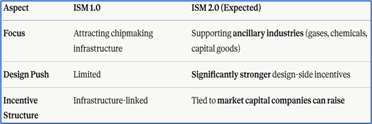
- ISM 2.0 reflects a more mature, ecosystem-wide approach — moving beyond just building plants to strengthening the entire semiconductor supply chain within India.
Conclusion
- This development highlights the fact that India is moving beyond basic chip assembly toward genuinely cutting-edge packaging technology that even advanced nations are only beginning to deploy.
- From a strategic perspective, investments by Lockheed Martin and Intel signal that India's semiconductor push is being taken seriously by global defence and technology majors.
- From an economic perspective, ISM is a textbook example of industrial policy — using state support to build strategic industries that the private sector alone would not develop fast enough.
- From a geopolitical perspective, reducing dependence on imported chips — especially from Taiwan and China — is directly tied to India's supply chain resilience and strategic autonomy.